
Applications of Boron Carbide in the Semiconductor Industry
Boron carbide (B₄C) features high temperature resistance, outstanding chemical inertness, plasma erosion resistance, low outgassing, high hardness and radiation resistance. It fits the high-temperature, vacuum and corrosive working conditions of wafer manufacturing, and serves as a key ceramic material for silicon chips and third-generation semiconductors.
1. Wafer Carrying Components for Vacuum Processes
- Boron carbide wafer trays, carriers and bases for high-temperature annealing, oxidation and diffusion furnaces. Low thermal expansion avoids deformation under high heat, ensuring uniform heating of wafers. Ultra-low alkali metal impurities prevent contamination of chip circuits. Compatible with silicon wafers, SiC and GaN substrates.
- Positioning baffles and guiding parts protect wafer edges from scratches in transit.
- Furnace internal fixtures, brackets and liners for LPCVD, diffusion furnaces. Resistant to corrosive process gases including HCl, chlorine and silane, stabilizing doping accuracy.
2. Etching & PVD/CVD Coating Equipment Parts
- Focus rings, edge rings and chamber liners for dry plasma etching. Resist halogen plasma bombardment and corrosion, maintaining stable etching uniformity and extending service life.
- Boron carbide sputtering targets: Coat protective films on circuits, MEMS devices and hard disk magnetic heads to boost wear resistance and anti-corrosion performance.
3. Precision Lapping & Polishing Abrasives
High-purity boron carbide micropowder (800#~5000#) is used for mirror finishing of silicon carbide, sapphire, AlN and GaN substrates. It delivers high grinding efficiency without heavy metal contamination, improving epitaxy yield.
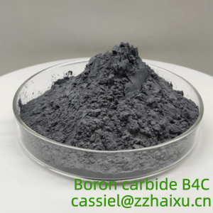
Boron carbide bonded abrasives dress diamond grinding wheels and grind packaging jigs.
4. Ion Implantation & Anti-radiation Components
Beam baffles, apertures and shielding plates for ion implanters withstand high-energy ion bombardment and prevent secondary wafer contamination.
Boron carbide fixtures are adopted for radiation-resistant chip testing.
5. Semiconductor Packaging Accessories
Wear-resistant mold inserts, dicing jigs and bonding fixtures keep dimensional stability during high-speed packaging, reducing wafer chipping and offset.
6. High-temperature Sensors & Thermocouple Sleeves
Boron carbide thermowell sleeves withstand temperatures above 2000℃ and resist corrosive process gases for furnace temperature measurement. It is also used as substrates for high-temperature pressure/temperature sensors.
7. Neutron Radiation Shielding
Boron carbide sheets and blocks provide neutron shielding for semiconductor radiation labs and wafer irradiation workshops, shielding wafers and precision equipment from neutron damage with no radioactive byproducts.
Key Advantages
- Resistant to hydrofluoric acid, halogen plasma and most process chemicals;
- Low impurity content avoids electrical failure of chips caused by ion pollution;
- Low thermal expansion guarantees stable processing dimensions at extreme temperatures;
- High hardness reduces abrasive shedding and particle defects on wafers.
Common Grades
High-purity boron carbide powder for sintering; narrow-distribution micropowder 1500#~5000# for polishing; boron-10 enriched powder for radiation shielding.